
3D Consideration of Stochastic EUV Resist Exposure Variations
Exploring through the third dimension sheds more light on stochastic variations

The sensitivity of EUV lithography to stochastic fluctuations in absorbed dose poses significant challenges. This article delves into the stochastic EUV exposure variations at different depths within the resist thickness, which ultimately affect pattern fidelity and yield.
When a resist layer, say 30 nm thick, absorbs EUV radiation, some light is absorbed in the top 10 nm, so that a reduced portion proceeds to the rest of the resist. Light continues to be absorbed in the middle 10 nm, leaving an even further reduced portion for the bottom 10 nm. Absorption results in release of electrons, which can travel further before activating chemical reactions, resulting in image blur (modeled with a Gaussian with sigma=3 nm here). Figure 1 shows the resulting exposure for two different types of EUV resists. The randomness in the distribution of electrons is modeled with a Poisson distribution for the electron number at each pixel (taken to be 0.5 nm).
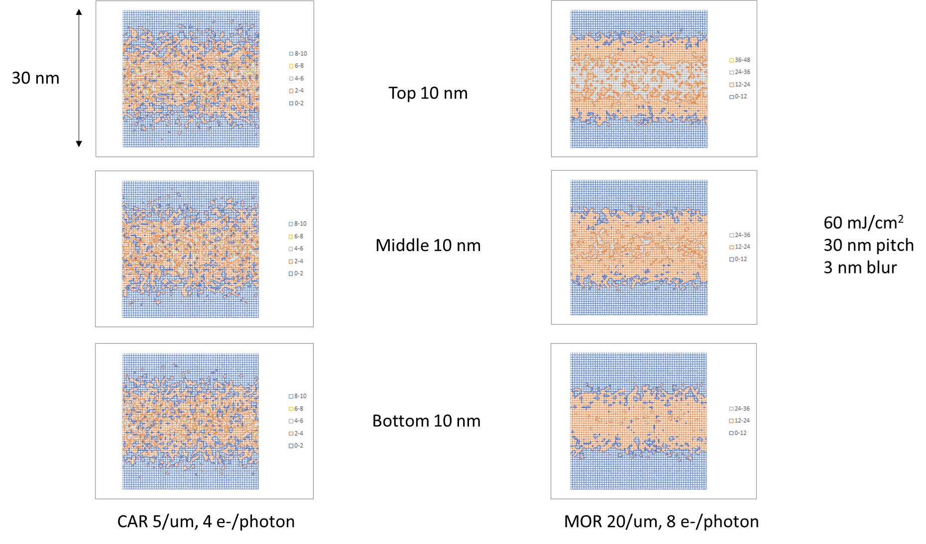
Figure 1. 30 nm pitch horizontal line exposed with 60 mJ/cm2 ideal dipole illumination, in CAR resist (left) and MOR resist (right), with absorption coefficients of 5/um and 20/um and electron quantum yields of 4 e-/photon and 8 e-/photon, respectively. The resist thickness is 30 nm. Top: Electrons/pixel in top 10 nm. Middle: Electrons/pixel in middle 10 nm. Bottom: Electrons/pixel in bottom 10 nm. Pixel size is 0.5 nm x 0.5 nm.
The chemically amplified resist (CAR) has lower absorption as well as electron quantum yield. As a result, the pixels show substantial noise at the printing threshold, with some occurring even outside the nominal 15 nm exposed region. This is also consistent with the reported reduction of post-development resist thickness with higher exposure dose [1], which unfortunately limits attempts to reduce the noise by increasing dose.
The metal oxide resist (MOR), on the other hand, shows a higher electron density, which would be less susceptible to noise. This is a consequence of both higher absorption and higher quantum yield [2]. However, the higher absorption has the drawback of significantly diminishing the number of photons reaching the bottom of the resist. This leads to an undesired undercut profile: the bottom resist linewidth is less than the top resist linewidth, as shown in Figure 1 on the right..
For holes or pillars, we can look at cross-section shape uniformity [3]. Figure 2 shows how the electron density may lead to shape variation as well as potentially even small net displacements at different depths through the cross-section of the exposed region.
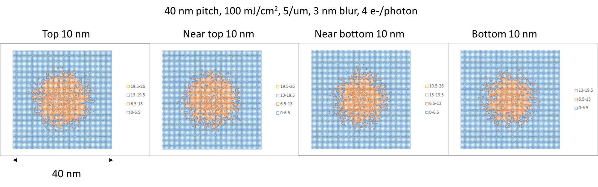
Figure 2. 40 nm pitch hole exposed with 100 mJ/cm2 ideal quadrupole illumination, in CAR resist, with absorption coefficient of 5/um and electron quantum yield of 4 e-/photon. The resist thickness is 40 nm. Electrons/pixel plotted at different resist depths. Pixel size is 0.5 nm x 0.5 nm.
While in these simulations, the extremely rough and perforated border between the pixels with electron density above and below the selected threshold value is obviously not defining the actual feature edge. For the case of the CAR, the resulting acid density also needs to be calculated (often by simplifying increasing the Gaussian blur sigma > 3nm) and similarly thresholded. We expect that the resist development process will consume the below-threshold areas of resist at some rate slower than the above-threshold areas. This should help smoothe out the pixelated roughness to form the usual edges we see.
It should be mentioned that electrons moving from one vertical slice to the next one above or below have not been considered here. The practical net effect would be a pixel in one slice going below the threshold while a pixel in the next slice above or below goes above the threshold. This is not expected to change the appearance of the outcome much, and is therefore not included. Also, as lateral motion is favored by the direction of the electric field of the EUV light [4], we would expect minimal vertical motion actually.
An obvious consequence of photon absorption in the upper portion of the resist is that the bottom 10 nm is more sensitive to stochastic variations. For example, the bottom 10 nm of the hole in Figure 2 gets 86% of the dose that the top 10 nm receives. There is a higher probability of failure to print some portion of the feature at the bottom. On the other hand, it may be argued that electrons from the underlayer [5] can make up for the deficit in electrons from fewer photons absorbed near the resist bottom. However, the image from these underlayer electrons is defocused relative to the resist image [6]. Also, the electrons are pre-scattered within the underlayer(s) before entering the resist. Exposure to these electrons in the resist will certainly incur additional blur.
We may also add more detail into our 3D model with different blurs at different depths in the resist (Figure 3).
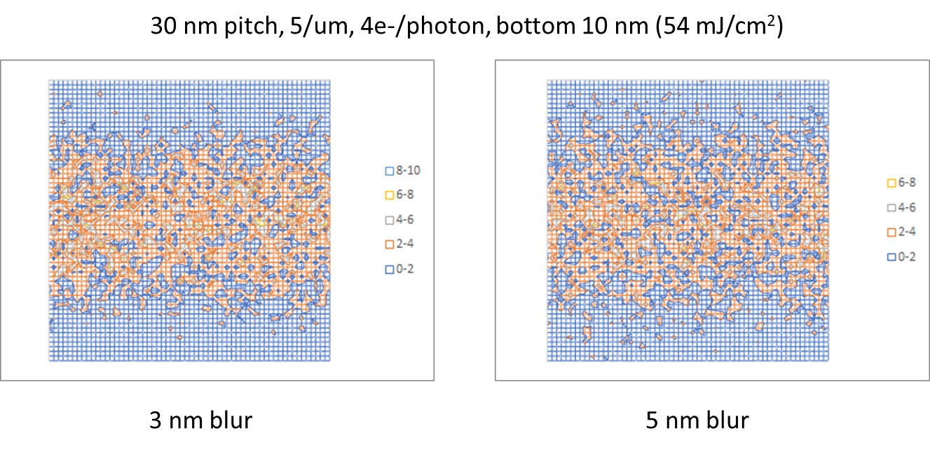
Figure 3. Blur impact on electrons/pixel in bottom 10 nm of 30 nm thick CAR resist exposed with 60 mJ/cm2 ideal dipole illumination (30 nm pitch), in CAR resist with absorption coefficients of 5/um and electron quantum yield of 4 e-/photon. Pixel size is 0.5 nm x 0.5 nm.
In short, considering the stochastic variation at different depths in the EUV resist provides more insight into the patterning outcome of EUV lithography.
References
[1] J. Severi et al., J. Micro/Nanopattern. Mater. Metrol. 21, 021207 (2022).
[2] Z. Belete et al., J. Micro/Nanopattern. Mater. Metrol. 20, 014801 (2021).
[3] J. J. Biafore et al., IEUVI TWG Resist, Oct. 2016, https://ieuvi.org/TWG/Resist/2016/20161023/09_biafore_kt.pdf.
[4] M. Kotera et al., Jpn. J. Appl. Phys. 47, 4944 (2008); I. E. McCarthy, Invited talk at The Fifth Atomic and Molecular Physics and Quantum Chemistry Meeting, 1989, https://inis.iaea.org/collection/NCLCollectionStore/_Public/22/036/22036447.pdf.
[5] T. Kozawa, Jpn. J. Appl. Phys. 62, 116502 (2023).
[6] F. Chen, https://www.linkedin.com/pulse/non-euv-exposures-euv-lithography-systems-provide-floor-chen-jymgc