
3nm Patterning Challenges with EUV Lithography

The 3nm node challenges EUV lithography to the extent that multipatterning is a necessity. Details are presented in the video below.
The TLDR summary:
EUV 0.33NA line patterning at 3nm minimum pitch (≤24 nm) is sensitive to pupil rotation, which will only allow narrow width chips to be exposed in a single mask scan.
The roundness of short line sections and line cut blocks makes them unfeasible for single exposure. In particular, dielectric reliability is jeopardized from the sharp tips left by rounded line cuts.
Stochastic variation severely affects the edge placement and quality for cuts and vias. This will force cuts and vias to be patterned with at least two exposures each.
The 6-track cell consequently needs to be patterned by multipatterning. However, LELE (Litho-Etch-Litho-Etch) splitting is susceptible to images shifting and edges moving asymmetrically through defocus.
It was not mentioned in the video but the line patterning itself is also severely affected by line edge roughness even for the EUV LELE arrangement with a dose of 55 mJ/cm2, due to the absorbed dose being much less.
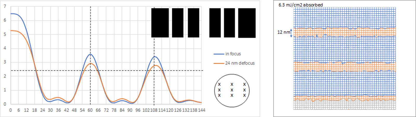
Left: One of the LELE exposures with an optimized illumination for 6-track cell with 24 nm minimum pitch. Right: Expected roughness for a dose of 55 mJ/cm2 (6.3 mJ/cm2 absorbed).
Instead of the LELE splitting, line patterning for the common 6-track cell metal layer will best be performed with 3 masks implementing single lines with the cell height (144 nm in this example) as pitch. These masks can in fact all be DUV exposures rather than EUV, but SADP would be used to define the narrowest lines, as in the case for the gates.