
A Molecular Origin for Stochastic Defectivity: Pinhole Probability Exponentially Increases in Thinner EUV Resists
A fundamental problem for increasing EUV NA

Thinner and thinner resists are expected to be used for printing smaller and smaller features with EUV. There are two reasons behind this. First, a move toward higher NA (from 0.33 to 0.55) significantly reduces EUV’s depth of focus [1]. Second, a smaller feature cannot support an aspect ratio greater than about 2 before there is a risk of collapse [2] or less effective etching (e.g., dry develop) [3]. Furthermore, EUV resists lose thickness with increasing dose due to outgassing [4,5].
Nanovoids [5] may form in resists after they are exposed and devloped, due to stochastic excessive deprotection or failure to completely crosslink. Using a Poisson process model, the probability that a pinhole defect forms in a volume of N voxels (or molecules) can be calculated assuming a threshold of defect formation of aN, i.e., a fraction a of the voxels or molecules are nanovoids, and an expected nanovoid fraction of b, i.e., bN voxels or molecules have been replaced by nanovoids. The formal result is the upper tail or complementary cumulative density function:
calculated using the probability mass function of the Poisson distribution [6]. An approximate expression using Stirling’s approximation was given in [5]. This can also be executed in Excel using the 1-POISSON.DIST(aN-1,bN,TRUE) formula.
With the number of voxels being a discrete variable, the CDF probability is not a truly monotically decreasing function of N. However, the overall trend follows an exponential dependence very closely. If we take a threshold of a=15% and an expected “natural” nanovoid fraction of 5%, the pinhole defect probability practically has an exponential dependence on N (Figure 1).
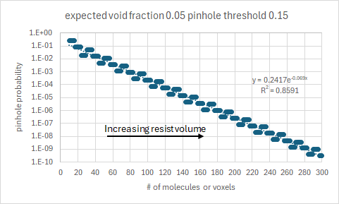
Figure 1. Pinhole defect probability vs. voxel number, with an expected void fraction of 5% and a defect threshold of 15%. An exponential fit is shown (dotted line).
For example, if we have a voxel or molecule size of 3 nm, an 18 nm x 18 nm area of resist that is 21 nm thick would constitute N = 6 x 6 x 7 = 252 voxels or molecules. In the scenario of Figure 1, we would get a defect probability of ~1e-8. For 36 nm pitch lines, this amounts to a defect density for 18 nm size defects of 1e-8/(36 nm x 18 nm), or over 1500 cm-2!
Thus, stochastic defectivity can not only originate from photon or electron number, but also molecular number. Resist feature volume can no longer scale due to the impact of molecular size on pinhole defect probability.
References
[1] F. Chen, Tip-to-Tip Limitations on Depth-of-Focus: When Higher NA Does Not Help.
[2] K. Yoshimoto et al., “Revisit Pattern Collapse for 14nm Node and Beyond,” Proc. SPIE 7972, 79720K (2011).
[3] J-H. Ting, J-C. Su, S. Su, “RIE lag in diffractive optical element etching,” Microel. Eng. 54, 315 (2000).
[4] F. Chen, Resist Loss Prohibits Elevated Doses.
[5] F. Chen, Stochastic Defectivity from EUV Resist Thinning: Why Higher Doses Make Things Worse.