Nanoparticles in the EUV-Induced Plasma: Another Possible Origin for Stochastic Defects in EUV Lithography
The most difficult EUV defect mechanism to control
Stochastic defects have been the bane of EUV lithography ever since it was used for printing wafers [1]. These defects appear as local regions which appear to be unexposed or incorrectly exposed, as well as misshapen or misplaced edges, which get worse for smaller features. The defects have been attributed to shot noise from low EUV photon absorption density [2], as well as blur [3]. However, the density of such defects has also been found to be as high as 1000/cm2 [4], even with doses higher than 150 mJ/cm2, pitches as large as 48 nm, and feature widths as large as 25 nm, where the dose noise and blur would have been expected to be suppressed. This suggests we need to look further for other significant mechanisms of stochastic defect generation.
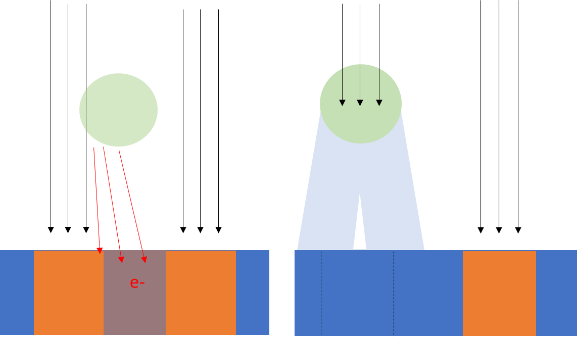
A recently observed phenomenon in EUV lithography systems is the EUV-induced plasma [5,6]. In EUV lithography systems, hydrogen gas is used to keep the multilayer mirror surfaces clean of carbon contamination and oxidation. This gas is ionized by the EUV light passing through it, forming a plasma, known as the EUV-induced plasma. The hydrogen plasma itself is capable of etching exposed carbon surfaces by chemical sputtering [7]. Plasmas are known for producing particles [7-9]. In particular, carbon that is chemically sputtered from the resist can redeposit as well as form particles, which can have sizes below 30 nm [9]. The particles will be negatively charged [8,10], while the EUV-illuminated resist surface would be positively charged [5,10], and gravity and gas flow also tend to push the particles toward the surface. Nanoparticles present near the resist surface or accumulated on the resist surface can affect the local exposure dose (see figure). It can be expected that features with a higher density than the nanoparticle density at or near the surface will be more vulnerable, while features sized much larger than the nanoparticles will be less affected.
Left: A nanoparticle located near the resist surface, releasing secondary electrons into the region between exposed features, causing a merging feature defect. Right: A nanoparticle located near the resist surface, reducing EUV exposure dose locally by shadowing, causing a missing feature defect. Note that an Arago bright spot [11] forms in the center of the shadow, but this is not enough to compensate the exposure.
Managing the stochastic defectivity therefore amounts to managing the particle generation and accumulation inside the EUV-induced plasma. This is an extremely daunting task, given the difficulty in even detecting all of them at ~10 nm resolution on the resist surface, without accidentally adding particles due to the detection equipment itself. However, without this action, EUV lithography users are truly operating blind.
References
[1] Peter de Bisschop et al., "Impact of stochastic effects on EUV printability limits", Proc. SPIE 9048, Extreme Ultraviolet (EUV) Lithography V, 904809 (17 April 2014); https://doi.org/10.1117/12.2047827
[2] Chris A. Mack, “Shot noise: a 100-year history, with applications to lithography,” J. Micro/Nanolith. MEMS MOEMS 17(4), 041002 (2018); https://doi.org/10.1117/1.JMM.17.4.041002.
[3] Hiroshi Fukuda, “Cascade and cluster of correlated reactions as causes of stochastic defects in extreme ultraviolet lithography,” J. Micro/Nanolith. MEMS MOEMS 19(2), 024601 (2020); https://doi.org/10.1117/1.JMM.19.2.024601.
[4] Vidyasagar Anantha et al., "Optical defect inspection solution for EUV stochastics detection," Proc. SPIE 11323, Extreme Ultraviolet (EUV) Lithography XI, 113231J (23 March 2020); https://doi.org/10.1117/12.2552452.
[5] Mark van de Kerkhof et al., “EUV-induced hydrogen plasma and particle release,” Radiation Effects and Defects in Solids, 177:5-6, 486-512 (2022); https://doi.org/10.1080/10420150.2022.2048657.
[6] Yao-Hung Huang, Chrong Jung Lin, and Ya-Chin King, “A study of hydrogen plasma-induced charging effect in EUV lithography systems,” Discover Nano, Volume 18, article number 22, (2023); https://doi.org/10.1186/s11671-023-03799-4.
[7] Kirill Bystrov et al., “Reorganization of graphite surfaces into carbon micro- and nanoparticles under high flux hydrogen plasma bombardment,” J. Vac. Sci. Technol. A 31, 011303 (2013); https://doi.org/10.1116/1.4769733.
[8] M. Kundrapu et al., “A model of carbon nanotube synthesis in arc discharge plasmas,” J. Phys. D: Appl. Phys. 45, 315305 (2024); https://doi.org/10.1088/0022-3727/45/31/315305.
[9] Kazunari Koga et al., “Nano-particle formation due to interaction between H2 plasma and carbon wall,” Thin Solid Films 506– 507, 656 – 659 (2006); https://doi.org/10.1016/j.tsf.2005.08.062.
[10] Mark van de Kerkhof et al., “Plasma-assisted Discharges and Charging in EUV-induced Plasma,” Journal of Micro/Nanopatterning Materials and Metrology 20(01), 013801 (2021); https://doi.org/10.1117/1.JMM.20.1.013801.


