
Revisiting Electron Noise in EUV Lithography: It's Pseudo-Poissonian After All!

In previous articles [1,2], I had focused on quantifying electron noise as a function of dose, and assessing the consequences. This turned out to be more equivocal than I expected. The statistics for treating the number of electrons as the product of electrons per photon and the number of photons (as I had done in the earlier articles) is fundamentally different from treating it as a sum of a varying number of electrons resulting from each photon, over the random number of all the photons.
Variance Calculations
The variance of a product of variables XY is given by Var (XY) = E[Y^2] Var (X) + (E[X])^2 Var (Y). Note that by symmetry, X and Y can be reversed in this expression. On the other hand, if we have a sum for i=1 to Y of independent, identically distributed variables Xi, the variance is given by E[Y] Var(X) + (E[X])^2 Var (Y); basically E[Y{ replaced E[Y^2] which appeared in Var (XY). For a Poisson distribution with mean value N, E[Y] = Var(Y) = N, while E[Y^2] = N + N^2. Since the standard deviation-to-mean ratio involves dividing the variance by N^2, the sum’s variance is inversely proportional to the square root of N, while the product XY’s variance contains a term that does not depend on N, meaning it plateaus for indefinitely high N. This led to the earlier observation of electron noise reaching an asymptotic nonzero limit at high doses, unlike the photon shot noise, which would approach zero [1,2].
The product XY is symmetric between X and Y but the sum for i=1 to Y of Xi fundamentally breaks the symmetry. This more accurately reflects the relationship between the absorbed photon and the subsequently released generations of secondary, tertiary, quaternary, etc. electrons. Therefore, we should replace the previous variance formula with the new one for the random sum.
We still assume a Poisson distribution for the absorbed photon number and a uniform interval distribution for the number of electrons released per photon and retained in the resist. Since the new variance is proportional to a Poisson variable, it is effectively pseudo-Poissonian. The variance is proportional to the mean absorbed photon number, so the standard deviation-to-mean ratio is inversely proportional to the square root of the mean absorbed photon number (Figure 1).
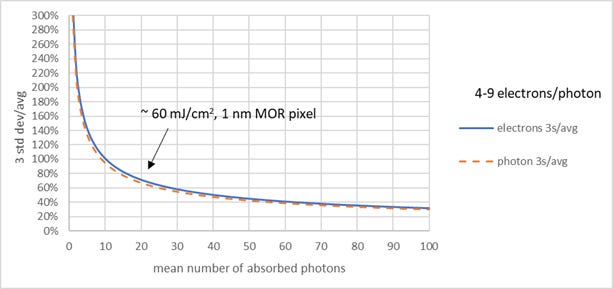
Figure 1. 3 sigma/avg noise for absorbed EUV photons and release electrons. Calculation is explained in text.
With X being the number of released electrons per absorbed EUV photon and distributed uniformly over the interval [p,q], E[X} is (p+q)/2 while Var(X) = E[X^2] - (E[X])^2. The mean of the square of the electron yield E[X^2] can be calculated as:
giving the result n2+p(n-1)+(n-1)(2n-1)/6, where n=q-p+1. This is typically much larger than Var(X) = (n2-1)/12. The variance of the electron number then becomes E[Y] Var(X) + (E[X])^2 Var (Y). With E[Y]=Var(Y)=N, this becomes N [(n^2-1)/12 + ((p+q)/2)^2], which is roughly N(E[X])^2. The standard deviation is roughly sqrt(N) E[X], while the mean is N E[X], so the electron noise 3s/avg is nearly the same as the photon shot noise, as apparent in Figure 1.
Pixel Exposure Error Probabilities
Since the statistics has been modified from the earlier product case, we need to revisit the exposure defect probabilities as well. The standard deviation and mean for the blurred electron number can be used to directly calculate the cumulative density function (CDF) relative to a given threshold number, assuming they describe a normal or near-normal distribution. This, in turn, can determine the probability that a given pixel is on the wrong side of the exposure threshold (Figure 2).
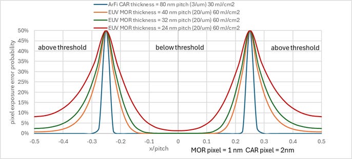
Figure 2. Pixel exposure error probability as a function of position. Blue: 80 nm pitch ArFi CAR targeting 40 nm trench in negative resist, 80 nm thickness, 30 mJ/cm2, s=5 nm Gaussian acid blur. Orange: 40 nm pitch 20 nm trench EUV MOR, 40 nm thickness, 60 mJ/cm2, electron blur given in [2]. Green: 32 nm pitch 16 nm trench EUV MOR, 32 nm thickness, 60 mJ/cm2, electron blur given in [2]. Red: 24 nm pitch 12 nm trench EUV MOR, 24 nm thickness, 60 mJ/cm2, electron blur given in [2]. The electron yield per EUV photon is 4-8.
By definition, the edge pixel exposure error probabilities are always 50%. Moving away from the edge, the exposure error probability drops toward zero, faster on the darker side of feature edge. ArF immersion clearly is less prone to stochastic exposure errors than EUV. The smaller EUV pitch is also more stochastic error-prone due to reduced contrast from electron blur.
Figure 3 shows the probability for a 3 nm long, 4 nm wide defect (negative resist removed) located at the line edge, with 40 nm half-pitch for ArFi with a negative CAR resist, and 40, 32, and 24 nm pitches for EUV with a metal oxide resist.
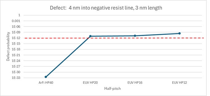
Figure 3. Defect probability for negative resist line edge defect, for the same exposure conditions as in Figure 2. 1e-12 corresponds to ~ 1/cm2 defect density [3].
A probability of 1e-12, corresponding to ~1/cm2 [3], is considered to be the upper limit. Even a 40 nm pitch would be still too defective, at 60 mJ/cm2, with 33 mJ/cm2 absorbed, and a 26% reduction in contrast from electron blur [4]. ArF immersion, on the other hand, has no issue of stochastic defectivity from the electron noise.
Conclusions
The main goals of this article are: (1) to overturn the previous finding that electron noise reaches a nonzero limit at indefinitely high dose, (2) to show the pseudo-Poissonian nature of electron noise, (3) to revisit the stochastic defect probabilities with the newly derived statistics. Although increased dose will reduce electron noise as well as photon shot noise, at current practical dose levels, the noise is still serious enough to drive stochastic defectivity.
Acknowledgment
I am grateful to Dr. Azat Latypov of Siemens EDA for a helpful exchange on LinkedIn, which led to revisiting this topic.
References
[1] F. Chen, How Secondary Electrons Worsen EUV Stochastics, Exposing EUV.
[2] F. Chen, Predicting Stochastic EUV Defect Density with Electron Noise and Resist Blur Models, Exposing EUV.
[3] P. Bisschop, “Stochastic effects in EUV lithography: random, local CD variability, and printing failures,” J. Micro/Nanolith. MEMS MOEMS 16, 041013 (2017).
[4] F. Chen, A Realistic Electron Blur Function Shape for EUV Resist Modeling, Exposing EUV.
Fred, brother, did I get this right? What you're saying in basic engineering terms is that these stochastic (random) defects are going to continue to happen? In fact if I extrapolate this, this is only going to get worse, due to the random behavior of protons and electrons and that there's nothing we can do about it, down at the 1nm level? (at least so far). Could you kindly set me right about this.