
Underlayer Electrons Enhance EUV Stochastic Defectivity

Recently, it was revealed that in EUV lithography, the image in a resist layer may not be primarily formed by EUV light focused in the layer but instead is substantially affected by electrons that have been backscattered from the layer underneath the resist, i.e., the underlayer [1-5]. In particular, the finding from Tokyo Electron (TEL) [3] shows that by changing the underlayer, the new underlayer’s electron exposure dominates the overall EUV resist exposure; the actual resist absorption actually becomes relatively minor. Aside from reducing the EUV dose to size by as much as a half, this also entails significant effects on the resist profile, CD (critical dimension), and even the defectivity.
As an additional source of electrons exposing the resist, the underlayer is expected to add more electron dose variability as well as blur (from defocus plus extended scattering volume) to the image. These effects will aggravate the already stochastic behavior of the EUV resist image. To visualize this, we first consider the 14 nm half-pitch case with metal oxide resist (Figure 1), where the underlayer allows the EUV dose to size to be halved. Conservatively, only a minor extra blur (Gaussian with 2.25 nm sigma) was used, but the range of electrons per photoelectron was assumed to increase from 5-9 to 10-18 due to the extra contribution from the underlayer.
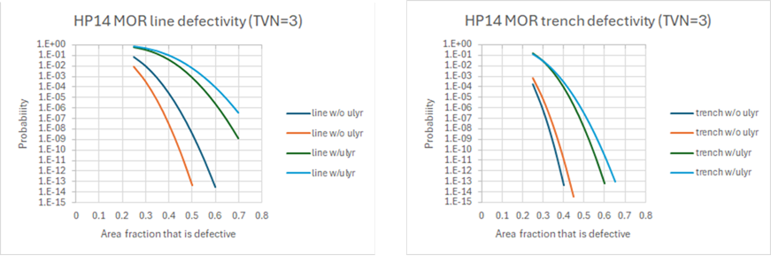
Figure 1. Comparison of stochastic defectivity between with and without underlayer for (left) resist lines and (right) spaces between resist lines. A 1:1 binary line-space pattern at 28 nm pitch was used to represent the mask pattern; two beam imaging was assumed. Absorbed dose: 30 mJ/cm2 w/o underlayer, 15 mJ/cm2 with underlayer. Resist electron blur: 1/3.2 nm exp(-r/3.2 nm)-0.14/0.448 nm exp(-r/0.448 nm). Extra blur from underlayer: Gaussian 2.25 nm sigma. Electrons/photoelectron: 5-9 (uniform distribution) w/o underlayer, 10-18 (uniform distribution) with underlayer. The threshold vicinity number (TVN) [6] is taken to be 3.
The probability that a given area fraction of the feature is defective, i.e., that a given fraction of image pixels has a threshold vicinity number [6] of 3, goes up exponentially in the presence of the underlayer. Note, though, that the resist line defectivity is already quite significant (1e-8 to 1e-13 at 50% defective area) even before the underlayer’s effect was included.
This result already hints that 28 nm pitch will require double patterning even with EUV. This could involve printing 14 nm lines on 56 nm pitch. However, even with less blur impact on this larger pitch, the stochastic defectivity gets much worse for this case (Figure 2), as the normalized image log-slope (NILS) is much smaller for 14 nm quarter-pitch than for 14 nm half-pitch.
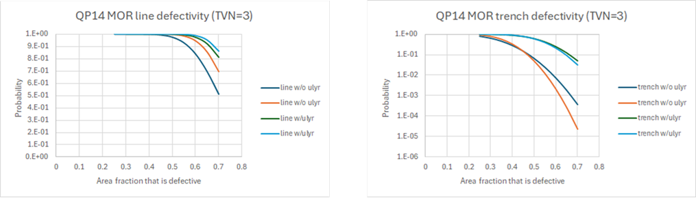
Figure 2. Comparison of stochastic defectivity between with and without underlayer for (left) 14 nm resist lines and (right) 14nm spaces between resist lines. A quarter-pitch binary pattern at 56 nm pitch was used to represent the mask pattern; two beam imaging was also assumed. Other conditions same as Figure 1.
Therefore, the only possibility left to enable double patterning would be to print 28 nm half-pitch features, then trim these down to 14 nm. In this case, EUV lithography is no longer the main determinant of critical dimension (CD); the subsequent trim etch becomes the key step. As shown in Figure 3, with a 28 nm half-pitch the stochastic defectivity has improved exponentially compared to 14 nm quarter-pitch or half-pitch features. However, in the presence of substantial electron exposure from the underlayer, a 28 nm resist line on 56 nm pitch can still have defect probability exceeding 1e-12, which corresponds to a defect density of ~ 1/cm2 defect density [6,7]. As expected, at these lowered levels, the defect density is highly fluctuating.
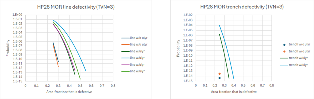
Figure 3. Comparison of stochastic defectivity between with and without underlayer for (left) resist lines and (right) spaces between resist lines. A 1:1 binary line-space pattern at 56 nm pitch was used to represent the mask pattern; two beam imaging was also assumed. Other conditions same as Figure 1.
To summarize, a substantial component of EUV resist exposure comes from the electrons emitted by the underlayer into the resist, rather than the EUV absorption itself. Furthermore, the additional electron exposure can significantly enhance stochastic defectivity.
References
[1] F. Chen, Estimating Underlayer Electron Exposure in EUV Lithography.
[2] F. Chen, EUV Resists are Getting Exposed by More than EUV Light.
[3] Y. Okumura et al., “Optimization of resist underlayer and novel development method for extreme ultraviolet,” Proc. SPIE 13983, 139832P (2026).
[4] S. Choi et al., “Understanding the Underlayer Effect using lithographic modeling,” Proc. SPIE 13983, 139831D (2026).
[5] H. Im et al., “Understanding the role of underlayers in enhancing EUV resist sensitivity,” Proc. SPIE 13428, 1342815 (2025).
[6] F. Chen, Explaining ppm-level Stochastic Defectivity in a 3nm Via EUV Lithography Process.
[7] P. Bisschop, “Stochastic effects in EUV lithography: random, local CD variability, and printing failures,” J. Micro/Nanolith. MEMS MOEMS 16, 041013 (2017).