
Explaining ppm-level Stochastic Defectivity in a 3nm Via EUV Lithography Process
The reason for EUV's erratic yield is also revealed.

In the past few years, there has been a growing effort to predict the probability of the occurrence of EUV stochastic defects [1-8]. As of mid-2025, the experimentally determined stochastic defectivity rate for a 3nm via layer (~22 nm CD on 40 nm pitch) was found to be at the ppm level (Figure 1) [6]. This is, in fact, many orders of magnitude higher than expected from basic estimates of pixel error probabilities from blur and electron and photon noise [7,8]. In this article, we will go over what drives the defectivity rates up so much.
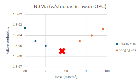
Figure 1. Missing and bridging via probabilities for a 3nm via layer (anchor: 40 nm pitch, 22 nm CD), as a function of dose [6]. A stochastics-aware OPC approach was used to reduce the defect probabilities. The red ‘X’ marks the projected minimum defect probability.
What makes an area defective?
The first consideration is the method of calculating defect probabilities. In Refs. [7,8], each pixel’s failure probability is solely determined by its exposure error probability, i.e., the probability that the resist solubility is in the wrong state. This is also considered independently of its neighbors. However, the product of the exposure error probabilities of all the pixels in the via is obviously too small, compared to a ppm.
More realistically, a pixel representing a molecular size would be affected by the status of its neighbor(s) as well [9]. Rather than the status of a pixel on its own, the solubility could be determined by the number of defectively activated pixels in its vicinity, defined as a 3-pixel by 3-pixel area centered on the pixel (Figure 2). Depending on the threshold vicinity number (TVN), the number of defective pixels determined this way could be much larger or smaller than the number of pixels which are themselves on the wrong side of the printing threshold. The TVN is just a way of giving an indication of how weakened a given location is from stochastic exposure in the immediate vicinity.
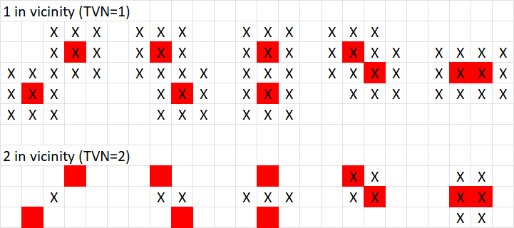
Figure 2. Top row: X’s mark pixels which are rendered defective by having at least one pixel on the wrong side of the printing threshold within their 3 x 3 vicinity. Bottom row: X’s mark pixels which are rendered defective by having at least two pixels on the wrong side of the printing threshold within their 3 x 3 vicinity.
As shown in Figure 2, if the TVN is 1, the final number of defective pixels could be several times more than the number of pixels on the wrong side of the printing threshold. On the other hand, if the TVN is 2, the final number can in individual cases will be less. As the TVN is raised to 3 or higher, we would expect the final number of defective pixels to decrease.
As we shall see below, the predicted stochastic defectivity is actually highly sensitive to the TVN.
Missing Via Probability
A missing via can be expected to arise when the number of defective pixels contained within the via is enough to occupy a sufficiently large enough fraction, e.g., 70% [6], of the via area. A 22 nm via on 40 nm pitch square array is modeled as the anchor feature for a 3nm via layer, as in [6]. A dose of 89 mJ/cm2 (based on Figure 1) is incident under quadrupole illumination (4-beam imaging) on 50 nm positive-tone chemically amplified resist (CAR), but only the bottom 40 nm remains to keep the image, due to resist loss increasing with dose [10] from outgassing [11] and other mechanisms. The electron yield per photon is modeled as a normal distribution with mean of 4.5 and standard deviation of 1, and the acid yield per electron is fixed at 1. The combined electron and acid blur is taken to reduce the contrast of a sinusoidal image by 48% for 40 nm pitch and 76% for 28 nm pitch.
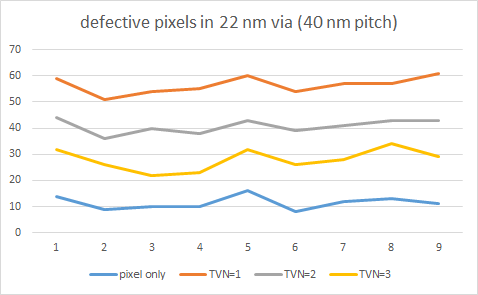
Figure 3. The number of defective pixels in a 22 nm via (40 nm pitch) decreases with increasing threshold vicinity number (TVN). Exposure and resist conditions given in text.
In Figure 3, we see that a threshold vicinity number of 1 gives the largest number of defective pixels in a 22 nm dense via, leading to the largest predicted probability of defectivity. Raising the threshold vicinity number decreases the number of defective pixels, as expected.
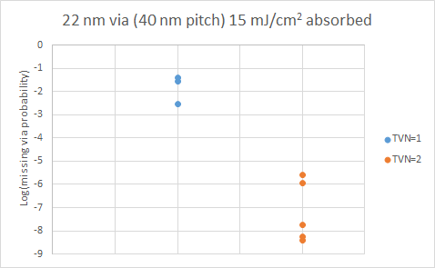
Figure 4. Missing via probability decreases exponentially with increasing TVN. Same conditions as in Figure 3.
Figure 4 shows the dependence of missing via probability on the threshold vicinity number. A TVN of 2 gives a much closer approach to the results of Ref. [6], yet it is interesting to note that for a given threshold vicinity number, the probability can vary over orders of magnitude. This hints at the erratic nature of EUV process yield [12]. This large variation is ultimately due to the many possible arrangements of pixels which are on the wrong side of the printing threshold, generally near the feature edge.
Via Bridging Probability
Via bridging can also be studied using the same approach as above, but now looking for pixels that are defectively deprotected (instead of not deprotected) in the dark area between vias. Under the same conditions, with TVN=2, the defect probabilities are comparable to what is shown at the crossover point “X” in Figure 1 (Figure 5).
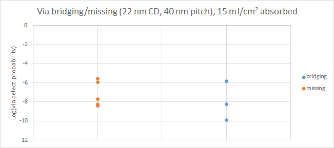
Figure 5. Bridging vs. missing via probability under the conditions of Figures 3 and 4.
How much does electron noise matter?
Loss of electrons from the EUV resist, as naturally expected with photoemission, can increase the local variation (sigma) in electron number, while decreasing the average. This can be expected to increase defect probability, but not with statistical significance (Figure 6).
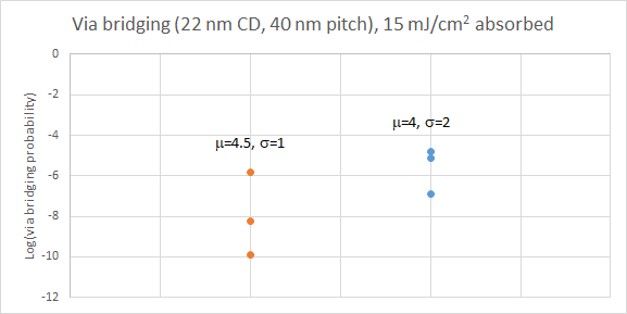
Figure 6. Increased electron noise affects the defect probability, but not with statistical significance in this case. Same conditions as in Figures 3-5.
Projection for MOR Process
It would be interesting to extend the TVN defectivity model to other resist processes. The metal oxide resist (MOR) is used for line/space patterns in the most advanced EUV lithography processes. The lower blur and higher absorption expected for MOR compared to CAR should lead to lower defect probabilities derived from photon shot noise. In this article, the blurs described in Ref. [7] were used.
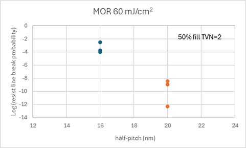
Figure 7. Resist line break probability for metal oxide resist (MOR) at 60 mJ/cm2(two-beam imaging). The thickness is taken to be equal to the pitch. The blur is assumed to reduce contrast by 26% for 40 nm pitch, 35% for 32 nm pitch. The electron number per photon is a random integer from 4 to 8 (uniform distribution).
In Figure 7, we assume if at least 50% of an 8 nm long strip of a 20 nm half-pitch resist line is defective (pixels over printing threshold), using the TVN=2 criterion, then it constitutes a broken resist line defect. This could be reasonable, since this corresponds to a 50% CD shrink, which for a via would result in it going missing [6]. We see that although for 40 nm pitch, the MOR line break probabilities tend to be lower than the missing via probabilities shown in Figure 4, it can still exceed 1e-12, corresponding to ~ 1/cm2 defect density [13]. Therefore, stochastic defectivity is still an overriding concern that limits the effective resolution of EUV.
References
[1] W. Gillijns et al., “Compact modeling of stochastics and application in OPC,” Proc. SPIE 12494, 124940J (2023).
[2] F. Chen, Non-EUV Exposures in EUV Lithography Systems Provide the Floor for Stochastic Defects in EUV Lithography, LinkedIn Pulse.
[3] S. Wang et al., “Towards efficient and accurate cost functions for EUVL stochastic-aware OPC correction and verification: via failure probability versus image and process variation band metrics,” Proc. SPIE 12953, 1295319 (2024).
[4] F. Chen, Nanoparticles in the EUV-Induced Plasma: Another Possible Origin for Stochastic Defects in EUV Lithography, Exposing EUV.
[5] F. Chen, Resist Loss Model for the EUV Stochastic Defectivity Cliffs, Exposing EUV.
[6] R. Meng et al., “Stochastic-Aware Compact OPC Model Validation for Reducing Failure Probability,” Proc. SPIE 13655, 1365507 (2025).
[7] F. Chen, Predicting Stochastic EUV Defect Density with Electron Noise and Resist Blur Models, Exposing EUV.
[8] F. Chen, How EUV Resist Blur and Dose-Induced Thinning Set the Stochastic Defectivity Floor, Exposing EUV.
[9] H. Fukuda, “Molecular cluster impact on EUV stochasticity,” Proc. SPIE 12953, 129530I (2024).
[10] F. Chen, Resist Loss Prohibits Elevated EUV Doses, Exposing EUV.
[11] F. Chen, EUV Resist Degradation with Outgassing at Higher Doses, Exposing EUV.
[12] Samsung Claims 60-70% Yields for its 3 nm Node | TechPowerUp; Samsung Electronics makes every effort to improve the yield of 'Exynos 2500'... 'Galaxy S25' in the second half of the year will be divided - ZDNet New Zealand
[13] P. Bisschop, “Stochastic effects in EUV lithography: random, local CD variability, and printing failures,” J. Micro/Nanolith. MEMS MOEMS 16, 041013 (2017).
After posting, this paper by Samsung and ASML from 2025 came to my attention, confirming the same >ppm-level results that I reported: https://www.spiedigitallibrary.org/conference-proceedings-of-spie/13426/134261Z/The-sub-ppm-level-of-stochastic-failure-model-for-random/10.1117/12.3050663.short Also observed two orders of magnitude failure probability variation across patterns at nominal condition. Defects with sub-ppm level failure probability could contribute to yield loss.
Again with the brains over brawn approach Fred. I was doing research on this very subject and whadayaknow....ol Fred Chen knows the real deal....Well done bud.