
Facing the Quantum Nature of EUV Lithography
Realistic doses are too low to treat EUV resist exposure classically like DUV

The topics of stochastics and blur in EUV lithography has been examined by myself for quite some time now [1,2], but I am happy to see that others are pursuing this direction seriously as well [3]. As advanced node half-pitch dimensions approach 10 nm and smaller, the size of molecules in the resist becomes impossible to ignore for adequate modeling [3,4]. In other words, EUV lithography must face its quantum nature.
Table 1 compares edge dose fluctuations for key cases for DUV, Low-NA EUV, and High-NA EUV lithography [5]. While for a standard dose of 30 mJ/cm2, DUV shows no significant dose fluctuations down to the smallest practical half-pitch, even at 60 mJ/cm2, EUV shows much greater than 50% fluctuation (3 sigma). Such a large dose fluctuation is expected to result in severe edge placement error, leading to roughness, linewidth errors, and/or feature placement errors. The key aggravating factors are: (1) an EUV photon has ~14 times the energy as a DUV photon, so that the photon density is already much less even at double the dose; (2) resist thickness scales with pitch, to avoid large aspect ratios for patterning, leading to reduced absorption; (3) EUV resists targeted for higher resolution would have smaller molecular sizes, leading to smaller photon collection area.
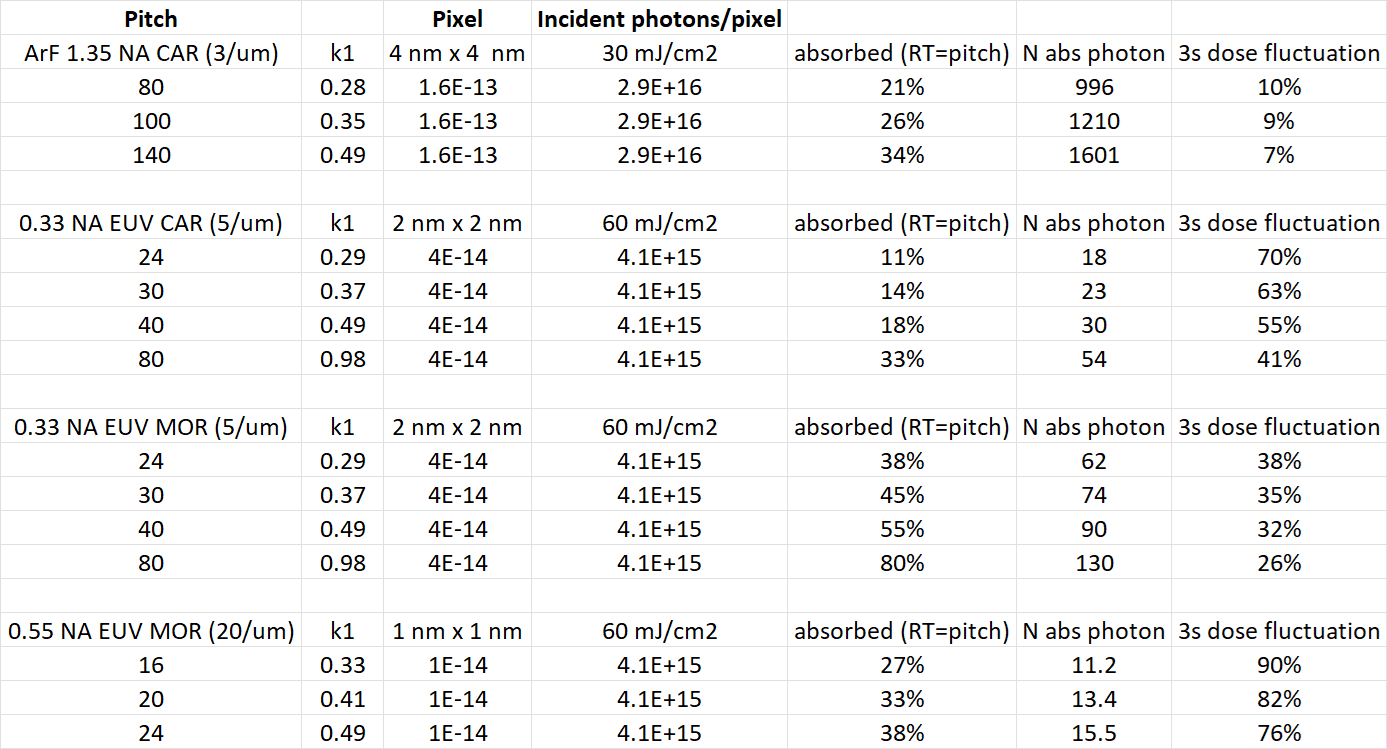
Table 1. Half-pitch edge dose fluctuations within a molecular pixel for DUV, Low-NA EUV, and High-NA EUV. An incident dose of 30 mJ/cm2 is assumed for DUV, 60 mJ/cm2 for EUV.
The photon absorption is not the final step in the resist exposure. An EUV photon will produce a photoelectron which then proceeds to migrate and produce more electrons, known as secondary electrons [2]. These electrons can in fact migrate distances greater than the molecular size [3]. As a result, the reaction of a molecule at a given location can be affected by the electrons resulting from absorption of photons at different locations, perhaps even several nanometers away [1].
Thus, the modeling needs to be addressed in stages. First, the absorption of EUV photons within the size of a molecule (~ 2nm [3,4]) needs to be addressed. Then, the effect of EUV absorption at different locations producing (random numbers of) secondary electrons all of which affect a given exposure location must also be taken into account. For chemically amplified resists, the acid blur should also be included for comprehensive modeling.
As a reference case, we will examine the 40 nm pitch (20 nm L/S binary grating) with a 0.33 NA EUV system. I’ll assume a chemically amplified resist with 40 nm thickness and absorption coefficient 5/um. Figure 1 shows the photon absorption density plot (top view), using 2 nm as the molecular pixel size, also representing the molecular size for the EUV resist. A 60 mJ/cm2 incident dose is assumed, which would result in 11 mJ/cm2 absorbed, averaged over the pitch. A threshold of 31 absorbed photons/nm2 would nominally correspond to the half-pitch linewidth.
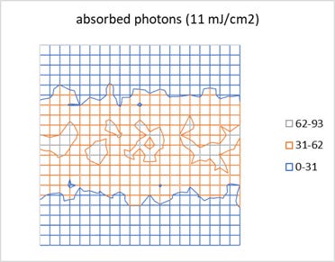
Figure 1. Absorbed photon density in 40 nm thick EUV resist with absorption coefficient 5/um and incident dose 60 mJ/cm2 (averaged over pitch) for imaging a 20 nm L/S binary grating. The pixel size is 2 nm.
Each photon is expected to produce up to 9 electrons [1], but can also be less. These electrons are not produced all at once but entail some electron migration. Thus, the electron blur parameter is often used to characterize this phenomenon. Contrary to the common assumption, we should not expect this to be uniform throughout the resist [1,6] due to the density inhomogeneity of the resist itself. Thus, a random number generator can be used to simulate the local electron blur parameter (Figure 2).
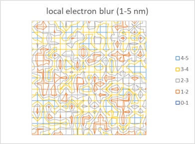
Figure 2. Electron blur is generated as a random number to represent local variation, due to natural material inhomogeneity.
The blur parameter actually describes the probability of finding an electron that has migrated a given distance. For the current example, we use the probability function shape shown in Figure 3, resulting from the difference of two exponential functions [7]. By convolving the local electron blur probability function with the absorbed photon density, then multiplying by the electron yield (taken to be a random number between 5 and 9), we can see the expected migrated electron density (Figure 4). Owing to the extra randomness of the electron yield added to the Poisson noise from photon absorption, the electron density plot includes enhanced non-uniformity.
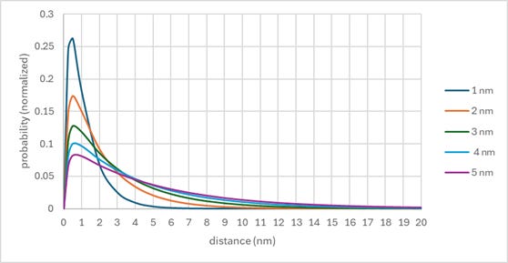
Figure 3. The shapes for the electron blur distance probability functions used in the modeling for this article. The shapes are generated from the difference of two exponential functions, one with the labeled long-range decay length (1-5 nm), and one with 0.2 nm decay length, so that the probability is zero at zero distance.
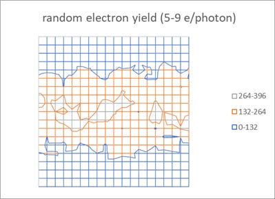
Figure 4. The migrated electron density is obtained by convolving the absorbed photon density of Figure 1 with the local electron blur probability functions (up to 8 nearest neighbor pixels) from Figures 2 and 3, then multiplying by the local random electron yield.
Since the resist is a chemically amplified resist, acids are produced by the electrons. These acids finally render resist molecules dissolvable in developer; this is known as deprotection [8]. The acids also diffuse, with the corresponding acid blur probability function taken to be a Gaussian. Figure 5 shows the final acid density plot after convolving a sigma=2.5 nm Gaussian acid blur probability function with the electron density. There is a smoothing effect from the acid blur, so some of the noise from the electron density plot seems to have diminished. However, there is still density variation that remains, since the seed of the acid generation is still random, i.e., the local electron density. Thus, the edge placement error is easily 10% of the linewidth.
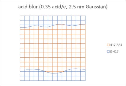
Figure 5. The acid density is obtained by convolving a 2.5 nm sigma Gaussian acid blur probability function with the migrated electron density of Figure 4 (in a 5 x 5 pixel area).
Smoothing with a larger sigma Gaussian would lead to further diminishing of the acid deprotection gradient; this would actually increase sensitivity to the level of deprotection, i.e., a smaller change in dose could wipe out the whole feature (Figure 6).
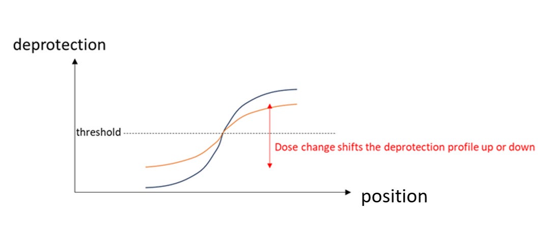
Figure 6. Smoothing by Gaussian blur with a larger sigma results in a less steep deprotection gradient (orange), which is more susceptible to wiping out features with dose changes. A smaller sigma would be less susceptible (blue).
The stochastic edge fluctuations begin to consume the whole feature as the exposed or unexposed linewidth shrinks (Figure 7). Essentially, the full-fledged stochastic defectivity shows up.
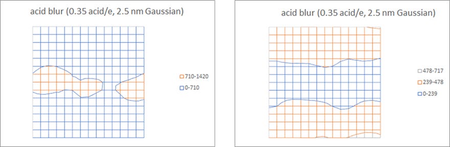
Figure 7. (Left) 10 nm exposed line on 40 nm pitch; (right) 10 nm unexposed line on 40 nm pitch, under same resist exposure conditions as Figure 1.
This level of edge fluctuation is a specific feature of EUV. The fundamental way to counteract this edge dose fluctuation is to increase the dose. To reduce it 10x, the dose needs to be increased 100x. Referring back to Table 1, to get the 3 sigma fluctuation down to 7%, the dose can easily approach 1000 mJ/cm2! That is clearly not feasible.
An alternative is to use double patterning, since doubling the pitch would enable 4-beam imaging, which can have higher normalized image log slope (NILS) than 2-beam imaging [9,10]. The dose would not have to be elevated as much. On the other hand, the 80 nm pitch exposure for double patterning is done more cost-effectively and quickly by DUV instead of EUV.
Moreover, 20 nm linewidths on 80 nm pitch with DUV 2-beam imaging at 30 mJ/cm2 look slightly smoother than optimized EUV 4-beam imaging at 60 mJ/cm2 (Figure 8). Besides the higher absorbed photon density per molecular pixel, there is no random electron yield component for DUV. Thus, DUV avoided the “perfect storm” that befell EUV [11], as it met its classical optical resolution limit before even approaching the molecular quantum limit.
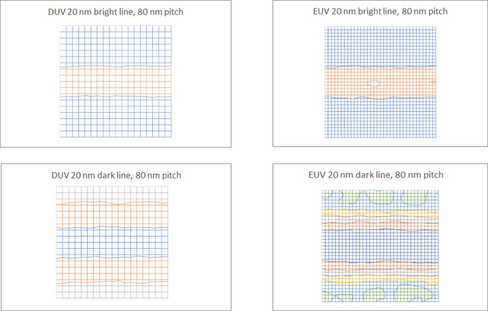
Figure 8. (Top left) 20 nm DUV exposed line on 80 nm pitch; (top right) 20 nm EUV exposed line on 80 nm pitch; (bottom left) 20 nm DUV unexposed line on 80 nm pitch; (bottom right) 20 nm EUV unexposed line on 80 nm pitch. The DUV (3/um) and EUV (5/um) chemically amplified resist thicknesses are both 40 nm.
References
[1] F. Chen, Impact of Varying Electron Blur and Yield on Stochastic Fluctuations in EUV Resist;
[2] F. Chen, Stochastic Effects Blur the Resolution Limit of EUV Lithography;
[3] H. Fukuda, “Statistics of EUV exposed nanopatterns: Photons to molecular dissolutions.” J. Appl. Phys. 137, 204902 (2025), and references therein; https://doi.org/10.1063/5.0254984.
[4] M. M. Sung et al., “Vertically tailored hybrid multilayer EUV photoresist with vertical molecular wire structure,” Proc. SPIE PC12953, PC129530K (2024).
[5] F. Chen, Stochastic EUV Resist Exposure at Molecular Scale
[6] G. Denbeaux et al., “Understanding EUV resist stochastic effects through surface roughness measurements,” IEUVI Resist TWG meeting, February 23, 2020.
[7] F. Chen, A Realistic Electron Blur Function Shape for EUV Resist Modeling
[8] S. H. Kang et al., “Effect of copolymer composition on acid-catalyzed deprotection reaction kinetics in model photoresists,” Polymer 47, 6293-6302 (2006); doi:10.1016/j.polymer.2006.07.003.
[9] C. Zahlten et al., “EUV optics portfolio extended: first high-NA systems delivered and showing excellent imaging results,” Proc. SPIE 13424, 134240Z (2025).
[10] F. Chen, High-NA Hard Sell: EUV Multipatterning Practices Revealed, Depth of Focus Not Mentioned
[11] F. Chen, A Perfect Storm for EUV Lithography
Electron noise dominates over EUV photon shot noise at higher doses: https://frederickchen.substack.com/p/how-secondary-electrons-worsen-euv
In this updated video presentation, 5 nm Gaussian acid blur smoothing is considered (rather than 2.5 nm): https://www.youtube.com/watch?v=Ogj1gz6kRrY